The Tale of Two Victure Baby Monitors: Part 1
NOTE: this series of blog post isnt all about security but more of a NoobieDog review. If i find security issues then great, if not then that is fine too. I have learnt something and maybe you have too!
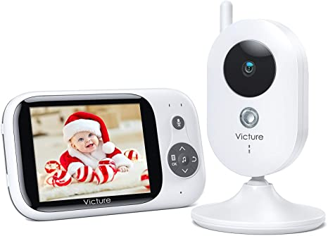
#1 Victure BM32 Baby Monitor
Spec:
3.2" LCD Display.
2.4GHz Wireless Digital Transmission.
Real-time video and audio.
Infrared Night Vision and Temperature Monitoring.
Two Way Talk.
930mAh Battery.
So initially this looks like a nice little playground to dig into, however it was quickly noted this was NOT the case.
Before the Unboxing:
Threat modeling:
Since this is an electronic device with very little tech capabilty the threat model is actually quite low, however it is a very personal device and has to be regarded in such manor too.
This device is designed to be able to see a baby/pet from another room (within 20 meters) and to be able to talk to them if needed!
The BIGGEST risk here is.. can somebody else SEE or SPEAK to the baby/pet...
If so, these are not regarded as "Secure" and probably wouldnt sell, however, in the RF world, there are a number of inherent flaws.
Interception:
Replay:
Jamming:
Impersonation:
Additional risks are:
Being able to view and see surronding objects/movement in the property.
Listening to surrounding sound of the transmitter.
Stop YOU listening/seeing your Baby/Pet
Minimal, but personal for sure!
Who would attack such a device..? Well..
Intel Agencies
Law enforcement
Criminals
News Agencies/Reporters
Why? well because if they know you have one of these, they may not need to enter your property or disturb things to place a listening/camera device...
Recon:
Before i even removed it from the box, i found the FCCID: 2AREL-BM32RX / 2AREL-BM32TX. One for the Reciever and the other for the Transmitter. However, these are just assigned to this "model" not the actual product internally. These are covered by a "Change in ID":
The original Grant for (2AQMY),under FCC ID: (2AQMY-ZR303TX)with a Grant Date of (08/16/2018)will remain in effect.An authorization letter from the original Grantee is attached.
So for this, we can use this FCCID: 2AQMY-ZR303RX & 2AQMY-ZR303TX
Links Here: https://fccid.io/2AREL-BM32T & https://fccid.io/2AREL-BM32RX
So what does this give us!
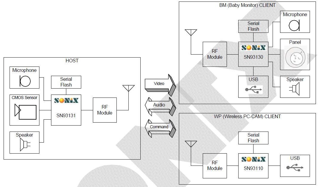
As usual, we get to see internal photos, some frequency measurements and testing, and sometimes if we are mega lucky, a working diagram!
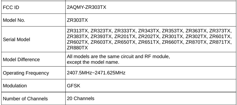
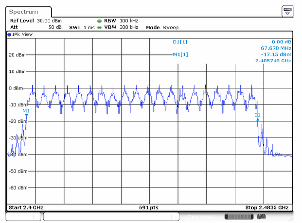
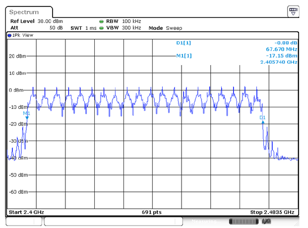
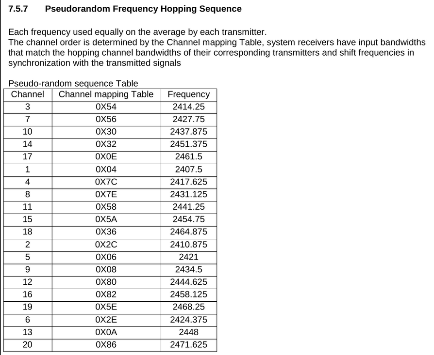
Nice, we have the freq, modulation and number of channels in use. From experiance this kinda already sets the tone for me, as this is frequency hopping solution and has a frequency span of 64Mhz... with a modulation of GFSK...
At this moment, i sighed... the reason, my HackRF doesnt have the capability to capture that much bandwidth AND i would need to work out the hopping routine to know what channel it was hopping too also the time between hops. Lets see if the RF report gives us this information.
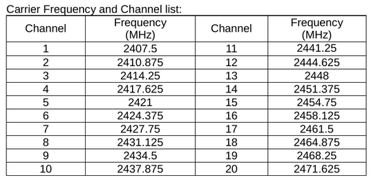
20 Channels nicely laid out for us!
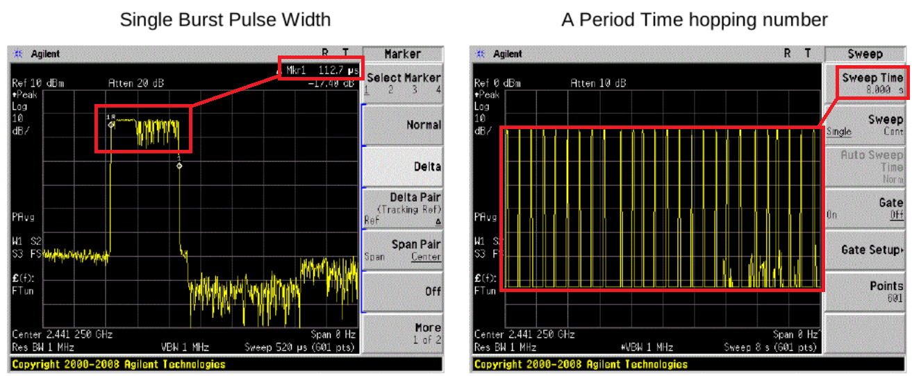
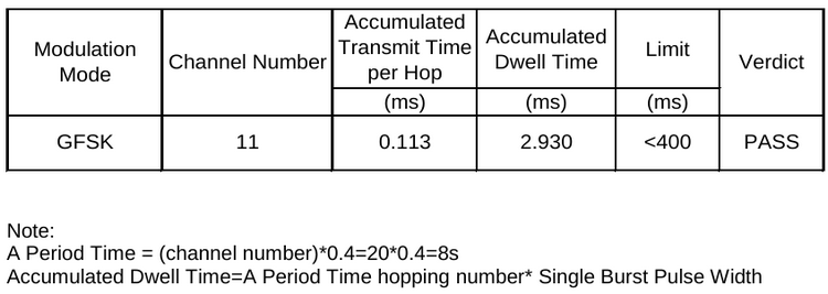
Timing for each channel transmission (112.7uS) and how long all 20 channels take (8s)
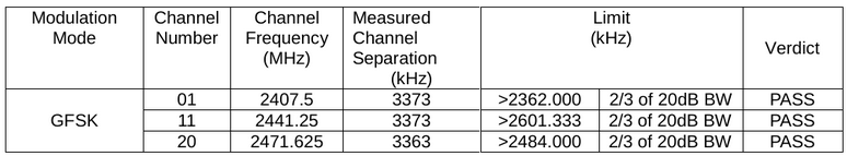
33kHz Channel Seperation
Consistent Channel shaping on each transmission.
One thing i didnt think about is this!
Ok well so this helps.
But in a world full of 2.4Ghz ISM Band transmissions (BLE, WIFI, ZigBee, OTHER) we can see overlap in the frequency range used on this device!
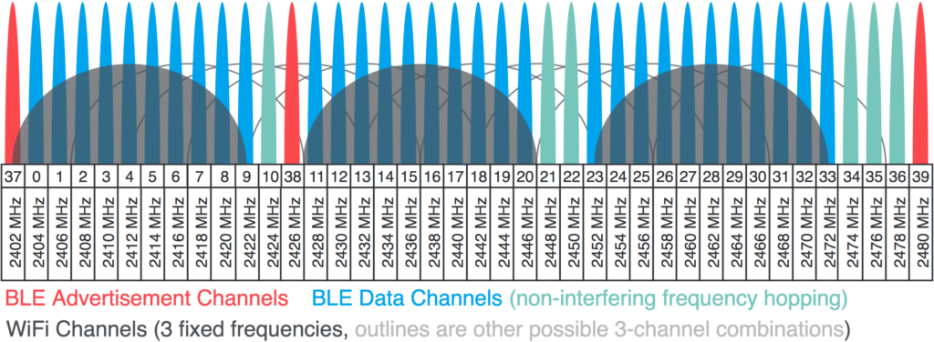
So 20 Channels, Spaced by 33kHz, used in a semi random order with a tonne of interference! AND with a modulation of GFSK!
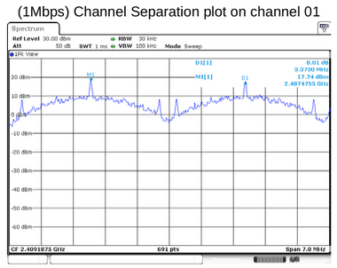
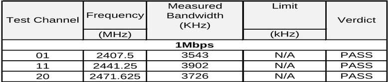
However, 3.5+khz per channel transmission bandwidth is more that capabile for the HackRF!
And the last peice of the puzzle we would need is the timing between channel hops to be able to even think about intercepting this device.
This information right here is why i love FCC and the info they release publically. It makes it easier for us in the reveng/security space to uncover these details quicker! So Thanks Mr FCC!
Lets open the box:
There are two devices in the box, quite nicely packaged and protected as you would expect. Very cheap and simplistic boxing.
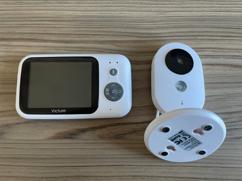
Both devices are minimal in design and have soft "cute" edges. The design its self has a "Baby-esq" feel to it. No sharp edges, soft to feel! The buttons are tactile to push and have a nice soft silicone coating.
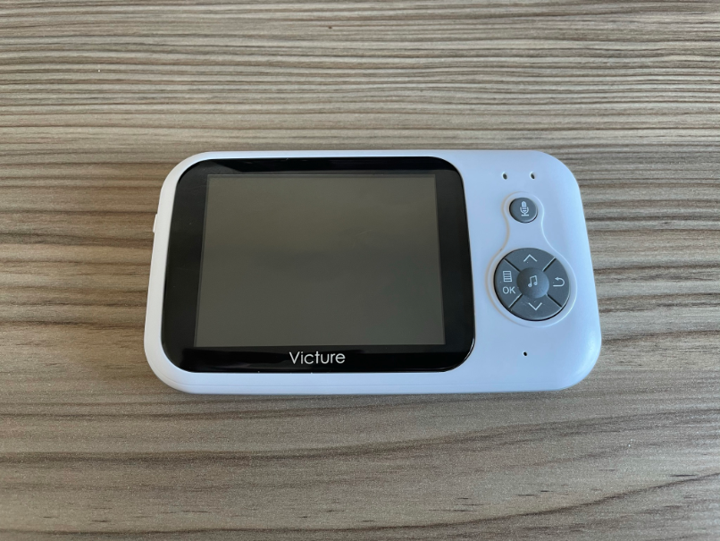
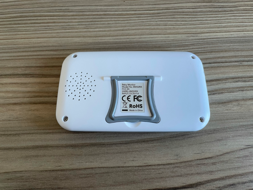
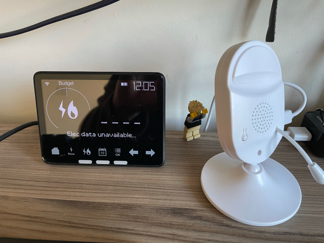
The Screen device... we shall call RX in some cases.. has a number of input buttons, a decent size screen and microphone/speaker for audio. Additionally it has a Micro USB connection for batter charging. It has a simple side button that turns the device on and off.
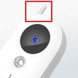
The Camera (AKA TX) is again smooth, rounded soft to feel. It obviously has the main camera, a IR LED and a microphone on the front. On the rear it has a Speaker, Reset button and a small antenna. It also has a power Micro USB connector on the side!
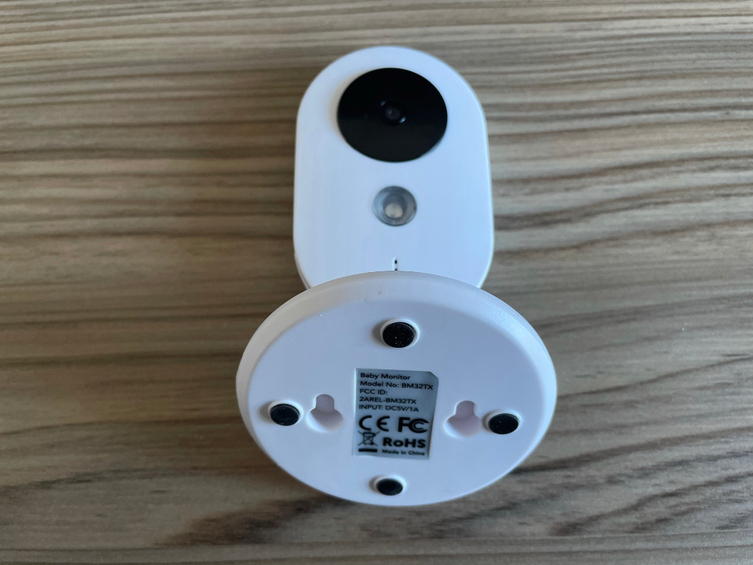
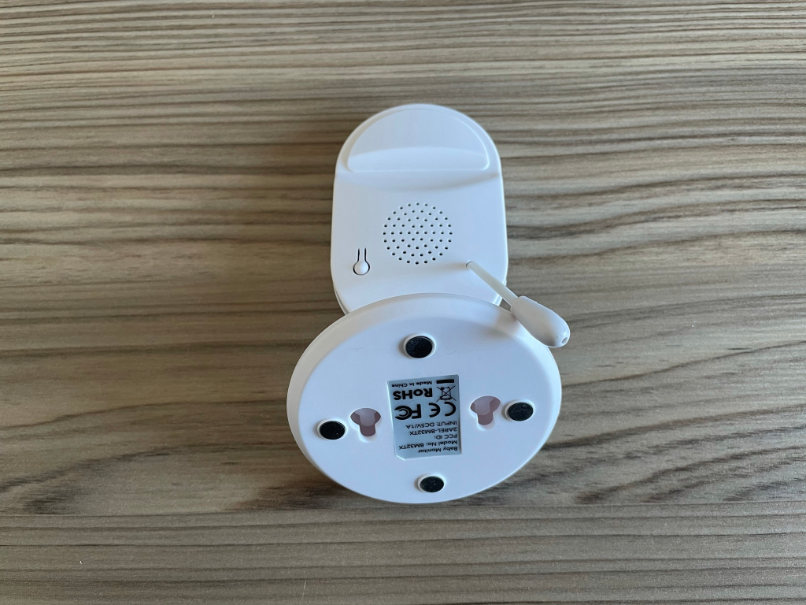
What i find strange is, the device has a "Antenna" on the top, however, this is not an antenna at all, and its just a empty, peice of plastic to look like an antenna! But then has a cable antenna coming out the back? a definate design flaw due to same pcb/hardware casing designs.
Powering UP:
Just plug the TX side into a 5v power supply or use the supplied power adaptor, turn on the screen and it works instantly with no setup! Nice
However in my mind, thats now a check list Item, how is it pairing and getting the timing so quick!
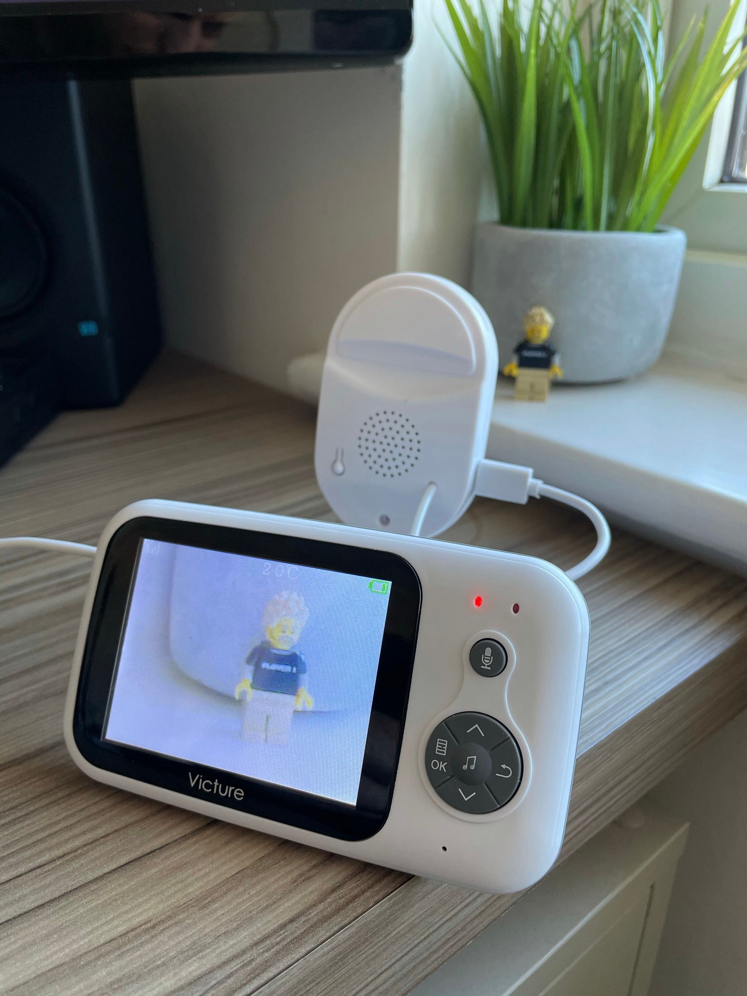
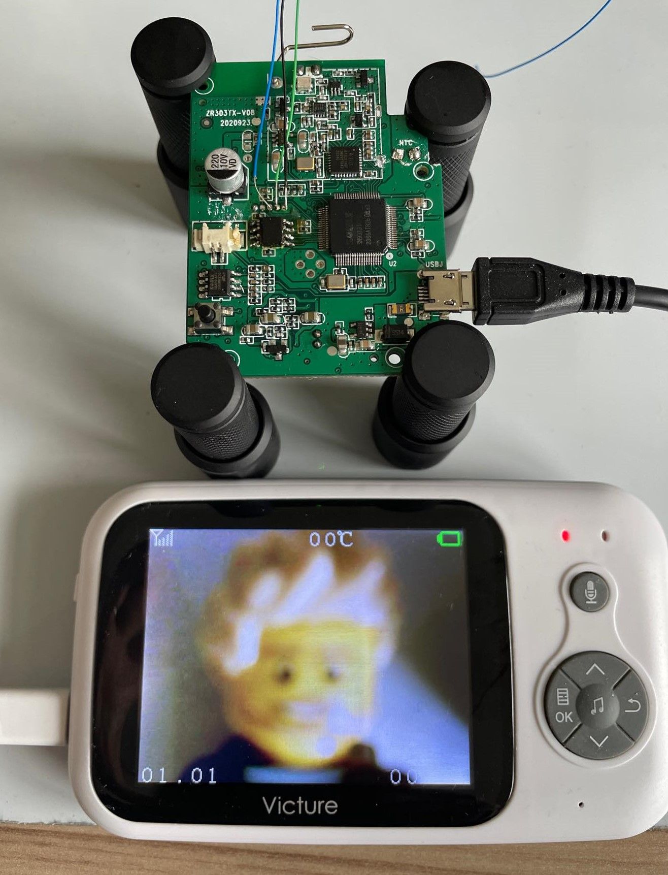
Essentially, with the RX device, you instantly see the camera feed and hear the sound from the TX device microphone. Working as expected!
On the RX, you do have the ability to "TALK" to the other end (TX). Parents could use this feature to be able to calm the baby/pet down from the other room.
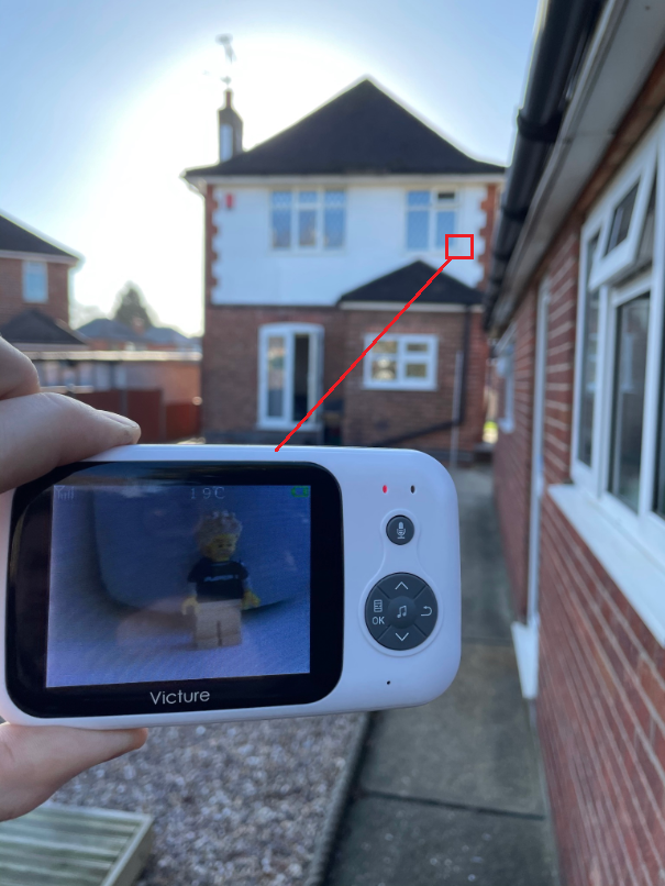
The range on this is quite impressive. Its about 20m-25m depending on obstructions (Line of sight, noise, etc...)
Talking about "NOISE", i noticed that when i turned the Baby Monitor on, it interfered with my Energy Smart Meter.
And if i unplugged it. The Smart meter came back!
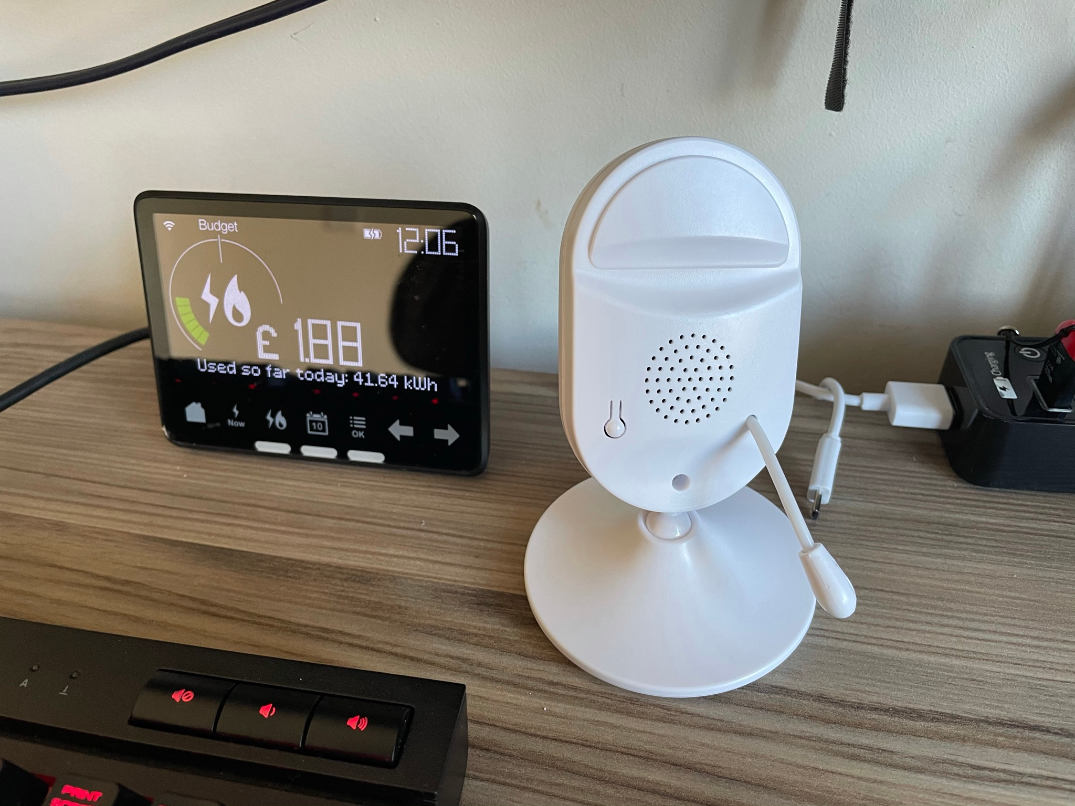
This is known as INTERFERENCE!
Radio Interference is where another set of radio signals interferer with another signal either disrupting it or causing a loss in service!
The frequencies in use by the Baby monitor bleed over the ones used by the Smart Meter, this stops the smart reader being able to talk to the other end! Simple!
Lets open them up!
Opening the Devices:
Transmitter (TX):
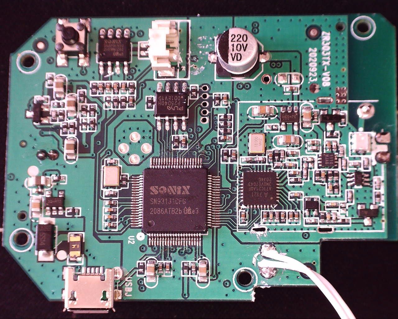
Clearly, the biggest thing that stands out is the DSP Chip (SONiX SN93131CFG). This Chipset has some really nice features.
- Use 2.4GHz ISM band FSK RF transceivers.
- Firmware protocol base adaptive FHSS (frequency hopping spreading spectrum). Meet telecommunication regulations.
- Built-in PLL for internal clock generation with input crystal frequency of 12MHz.
- Using external serial flash to store customized code and data.
- Path delay from Tx camera to Rx display less than 0.1 second for video and audio.
- 8080-CPU interface.
- Built-in 4 of 10 bit, 8K/16K sampling rate ADC for microphone, AD key, battery detection and general purpose analog input.
- Built-in 10 bit, 8K/16K sampling rate DAC for analog audio output.
- Support GPIO and PWM pin for local or remote control.
- Max. 8 selectable pins for GPIO and PWM.
- Support multiple ID for security.
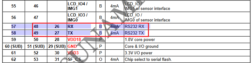
So looking through the Data Sheet (https://datasheetspdf.com/pdf-file/1089228/Sonix/SN93300/1) there are a number of pins that excite me
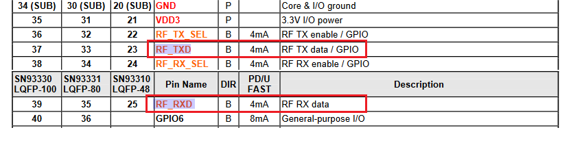
These pins (33, 35 are the RF Data pins.. These are important)
And these tell me we may be able to get a UART console ;)
Moving on to the other chipsets on the board, we can see that the Main DSP chip sends its RF data to an RF module!
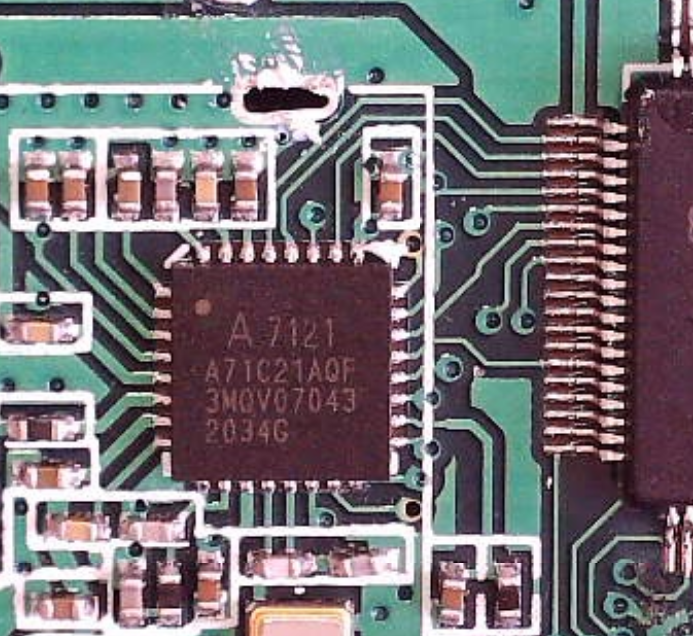
This RF Module is an A7121 2.4GHz GFSK Transceiver
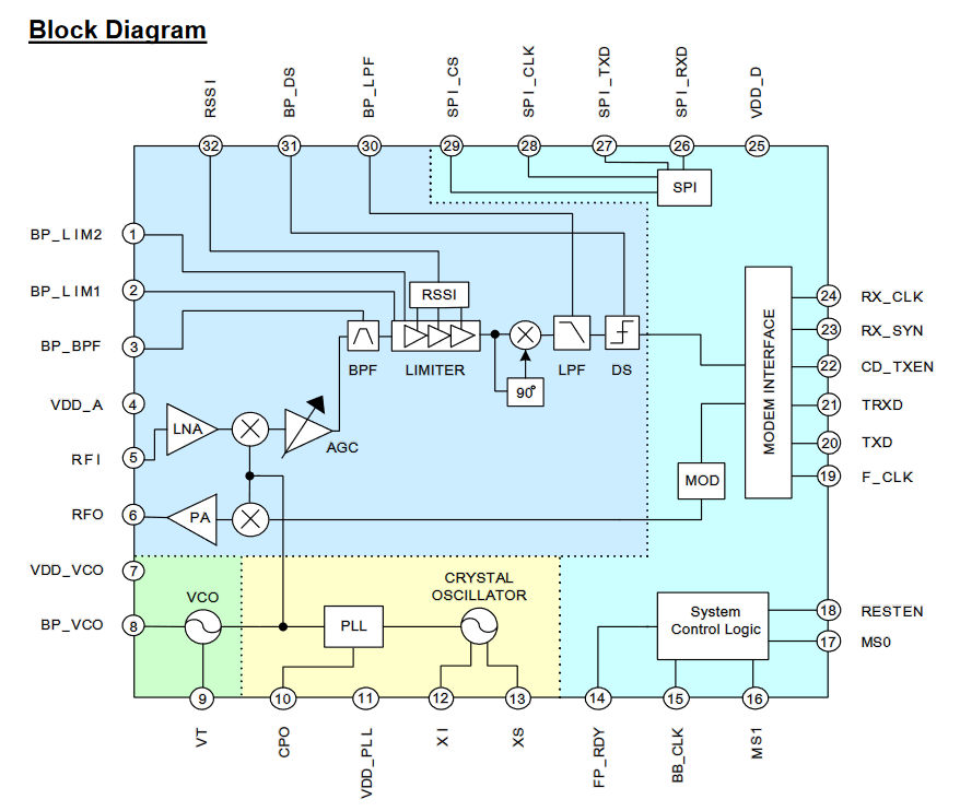
More information can be found here: https://github.com/zeza/gnuradio-rc-testcode/tree/master/doc/amiccom/A7122-pdf
Moving around the PCB, we can see another chip.
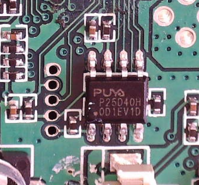
This is a PUYA P23D40H 4MB SPI Flash module.. Datasheet here: https://pdf1.alldatasheet.com/datasheet-pdf/view/1150759/PUYA/P25Q40H.html
Yes we are going to extract this!
Next to the SPI Flash is a 5 Pin through hole header. Im hoping this is for UART!
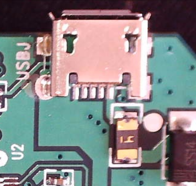
Next up, is the USB connector, Simply, this is used for power only. The Data lines are not even used on either side!
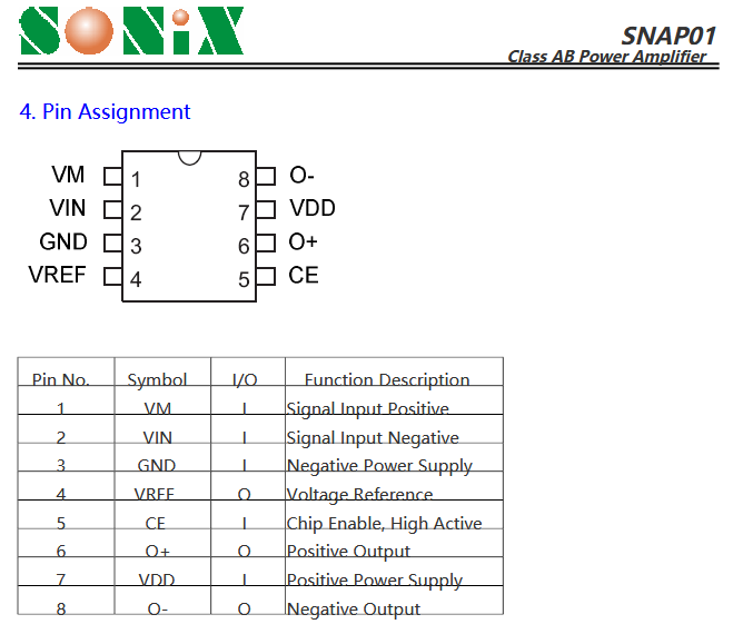
The only other Chip on the front side is this one
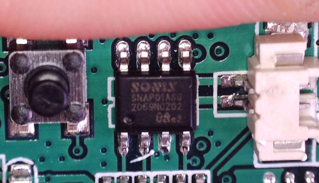
Its a SONiX SNAP01ASG - SONix Speaker Driver
Moving on to the front side of the PCB gives us some more of the features of the camera.
It has a Photo diode to sense Day/Night time.
It has a Camera on Ribon Cable.
There is a IR LED and a Microphone
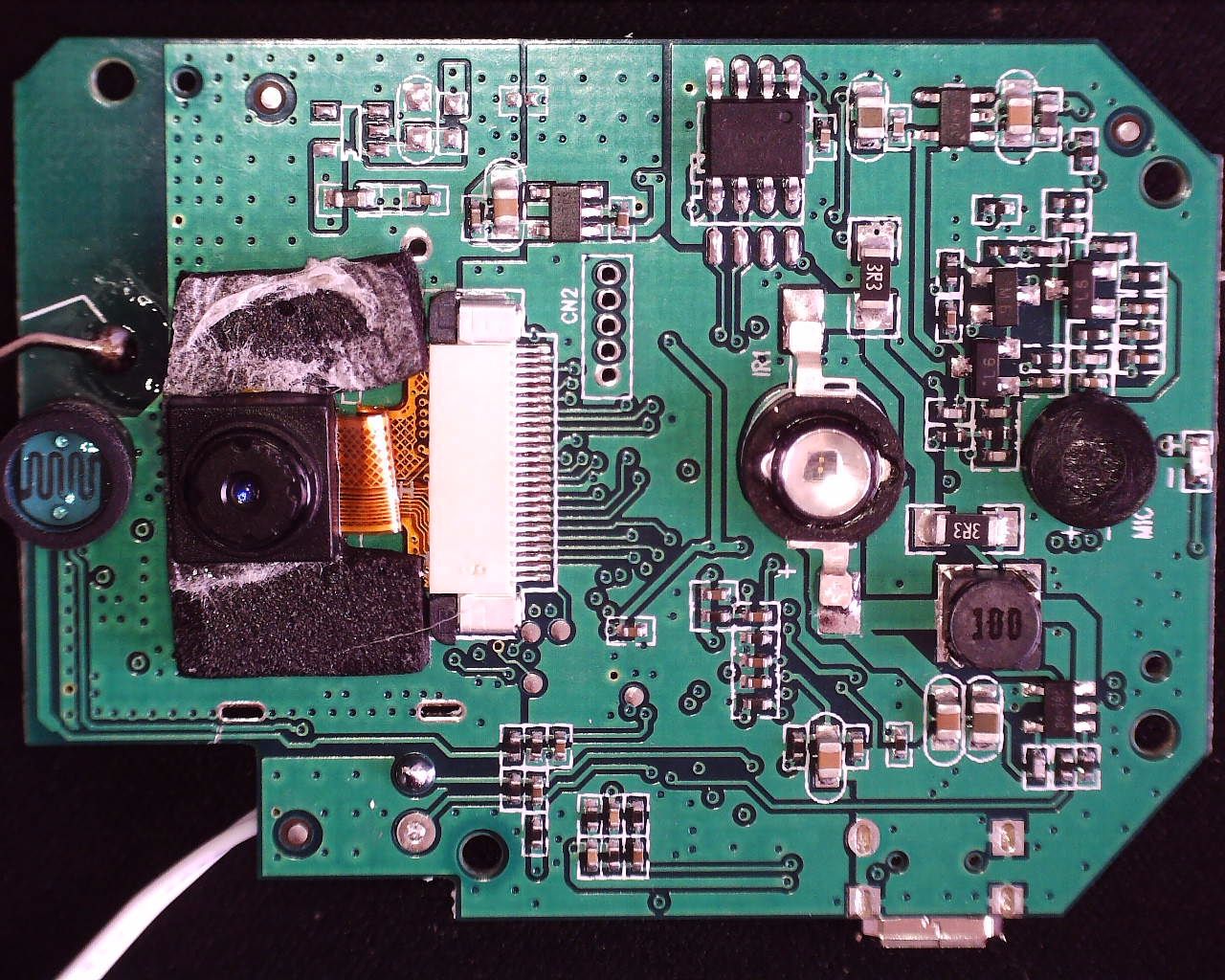
There is an SOP 8 IC that isnt quite obvious!
But honestly, non of this is particulary as interesting as the back side.
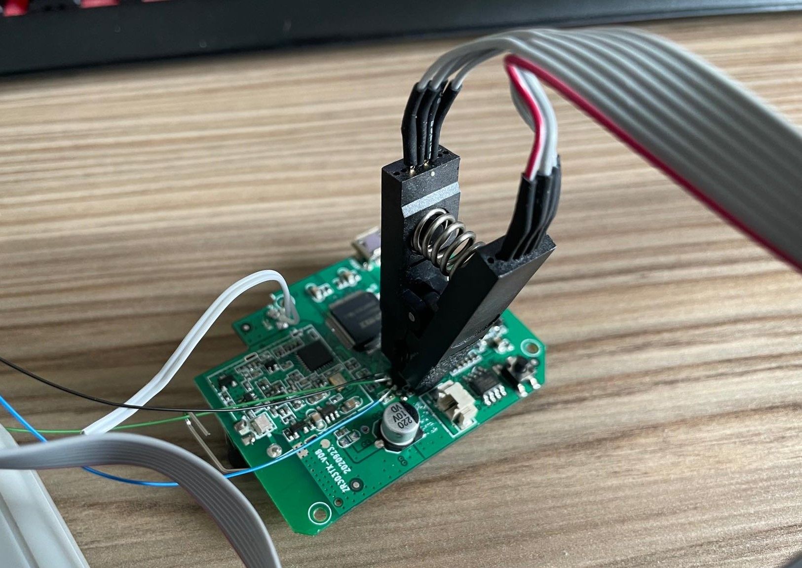
The Test Headers: TX
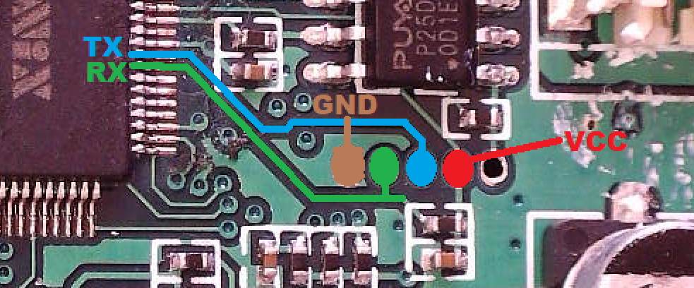
Lets see if we can get something from these pins with the Saleae
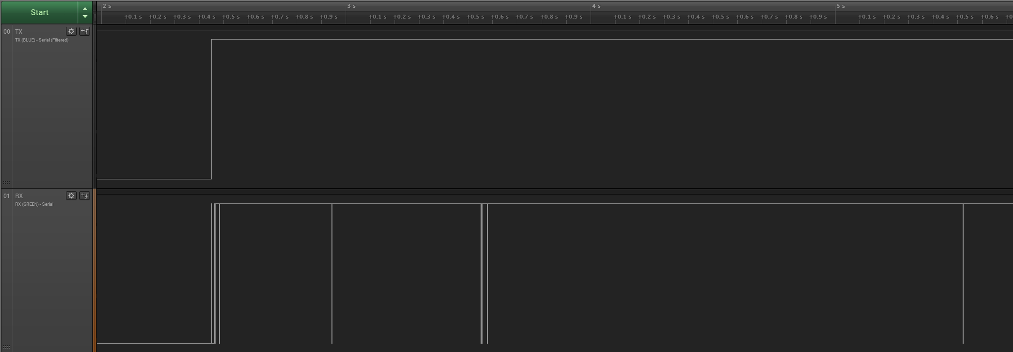
winner so there is something, lets take a closer looksie
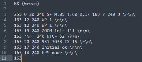
Interesting that its showing debug info on startup. However im not seeing any interface for a console so to speak.
The SPI Flash: TX
Lets pull the SPI flash and have a look at that... Remember, the more we know.. the further we go!
As always, i try the SOP8 Clip first, it never works. I find that when you power the chip from these clips, its also powering some of the other components, that causes the SPI to be locked as its already being read by something else. You can lift/seperate the Vcc pin if you like but i find it easier to remove all together!
So a desolder and it reads fine.
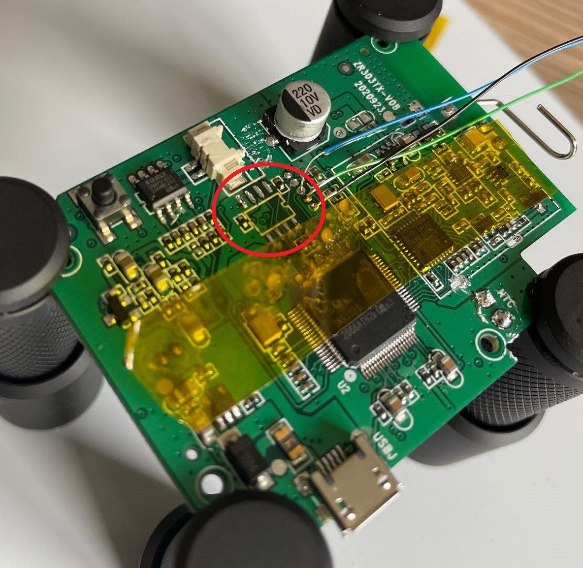
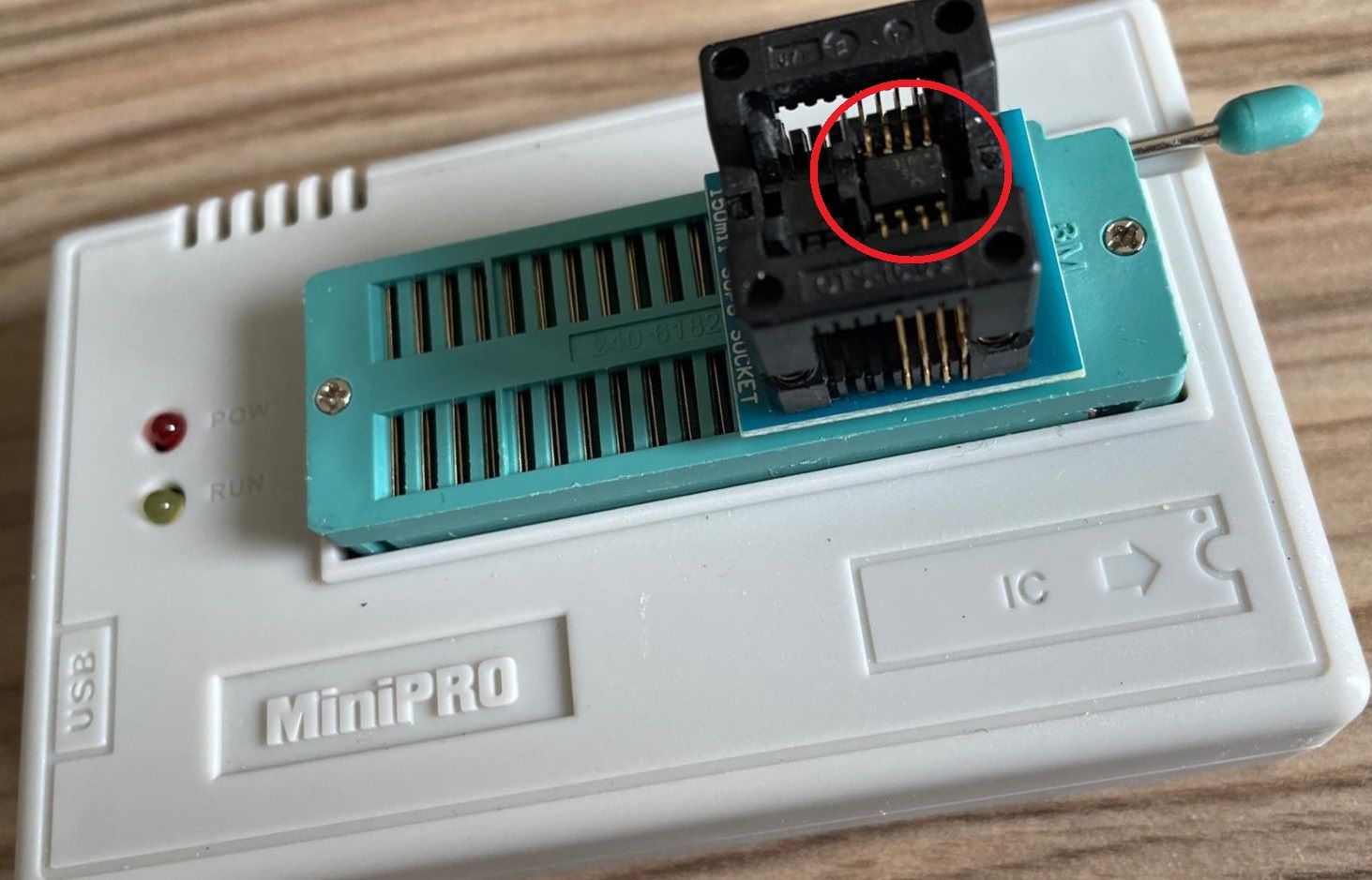
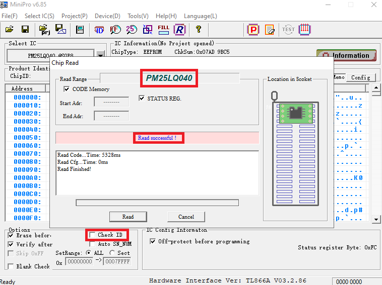
By disableing the "Check ID" on a chip read, it read the SPI flash fine. Most SPI are the same so you can pretty much use any that are on offer ;)
Lets see whats inside this flash dump!
First up "Strings"
We can see some simularities in the flash dump and the UART output! interesting but nothing that stands out really.
Lets solder the SPI flash back on and make sure it still works ok!
Since there is no user actions with the hardware so to speak, no uart console, nothing fancy in the SPI flash, complex RF signals and well a very basic piece of kit... where do we go from here!
Well, we havent looked at the RX side of things, so lets open it up and see whats inside...
Receiver (RX):
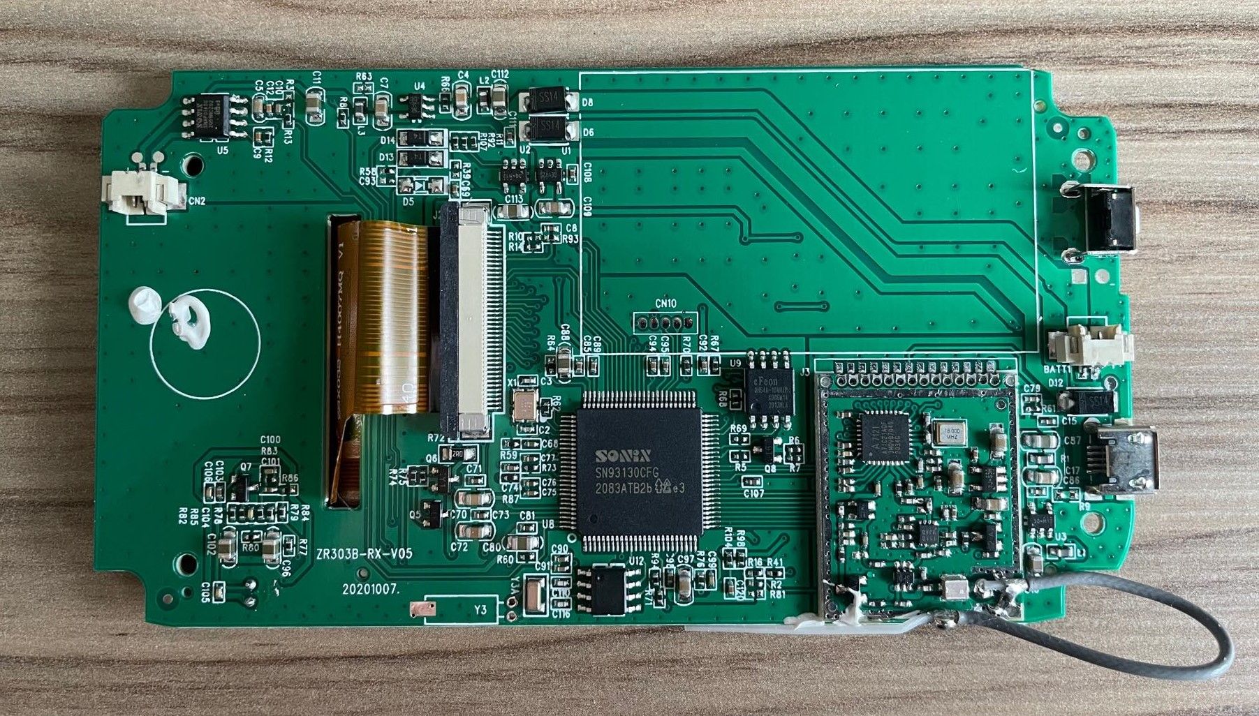
In reality, there really isnt much difference apart from the obvious screen, buttons, but all the internal components are near identical. Its interesting to see that they used a daughterboard for the A7121 Chip set module. The Sonix SN93130CFG chip pretty much controls everything.
There is another set of what look like UART pins, so i will get another capture from that too!
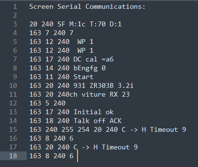
The UART output of the screen device (RX) has a little more info, see how its timing out due to the cam (TX) not being turned on.
Also i took note of the SPI Flash on the RX, its a EN25Q64A by cFeon (https://datasheetspdf.com/pdf-file/1347145/EON/EN25QH64A/1) a 64 Megabit 3V Serial Flash Memory.
The interesting question here is, why choose this over the other SPI they already used. Also the size is substantially different!
After extracting the flash from the RX (6mb in total) i now understand why they use a big ol flash... they are storing the image codes on the SPI for say, battery, text, logo, menu etc... that all takes space!
Secondly, there is alot more interactive based functions on the screen device (RX) so there generally will be more in the flash!
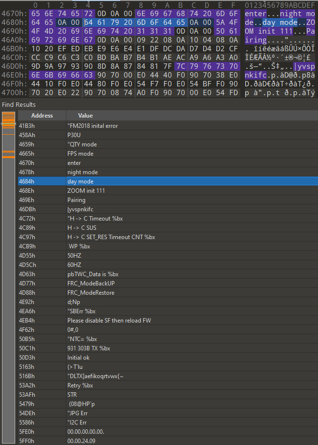
Lets have a look at the "Strings"
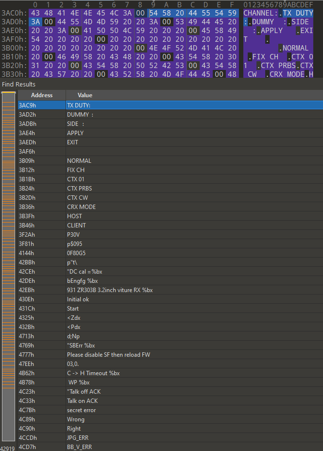
One thing that stands out is this!
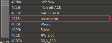
"secret error"
This is and will be written per device set, so hopefully each baby monitor, the secret should be different!
we need to see if we can get the secret key!
In the Datasheet for the Sonix SN933 chipsets, it states
Using external serial flash to store customized code and data.
So, for me, the secret key and code is stored on the SPI Flash. Interesting, and that would suggest why there is no debug/programming pins on the Sonix Chipset
Ive been messing with the firmware's to see what differences they have! WOW this is going to be messy
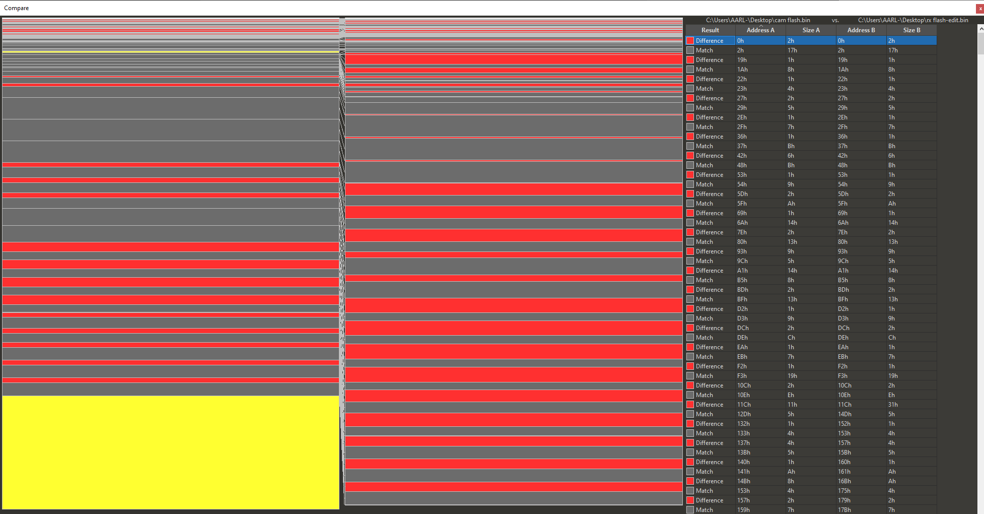
So YES there are some repition of CODE/DATA in both SPI Flash dumps, but there is far to much noise at the same time, this make it really hard to decypher.
Lets put them back together, and start looking at the RF side of things! Watch out for Part 2 Soon